- 您现在的位置:买卖IC网 > Sheet目录17378 > ADP2105-1.8-EVALZ (Analog Devices Inc)BOARD EVALUATION ADP2105Z 1.8V
�� �
�
�ADP2105/ADP2106/ADP2107�
�Table� 8.� Minimum� Inductor� Value� for� Common� Output�
�Voltage� Options� for� the� ADP2107� (2� A)�
�V� IN�
�18�
�17�
�16�
�15�
�14�
�13�
�Data� Sheet�
�V� OUT�
�1.2� V�
�1.5� V�
�1.8� V�
�2.5� V�
�3.3� V�
�2.7� V�
�0.83� μH�
�0.99� μH�
�1.19� μH�
�1.65� μH�
�2.18� μH�
�3.6� V�
�1.00� μH�
�1.09� μH�
�1.19� μH�
�1.65� μH�
�2.18� μH�
�4.2� V�
�1.07� μH�
�1.21� μH�
�1.29� μH�
�1.65� μH�
�2.18� μH�
�5.5� V�
�1.17� μH�
�1.36� μH�
�1.51� μH�
�1.70� μH�
�2.18� μH�
�12�
�11�
�10�
�9�
�8�
�7�
�6�
�5�
�4�
�3�
�?� Output� Capacitor� =�
�≈� 20� μ� F�
�Table� 9.� Inductor� Recommendations� for� the� ADP2105/�
�ADP2106/ADP2107�
�Small-Sized� Inductors� Large-Sized� Inductors�
�Vendor� (<� 5� mm� � 5� mm)� (>� 5� mm� � 5� mm)�
�Sumida� CDRH2D14,� 3D16,� CDRH4D18,� 4D22,�
�3D28� 4D28,� 5D18,� 6D12�
�Toko� 1069AS-DB3018,� D52LC,� D518LC,�
�1098AS-DE2812,� D62LCB�
�1070AS-DB3020�
�Coilcraft� LPS3015,� LPS4012,� DO1605T�
�DO3314�
�Cooper� SD3110,� SD3112,� SD10,� SD12,� SD14,� SD52�
�Bussmann� SD3114,� SD3118,�
�SD3812,� SD3814�
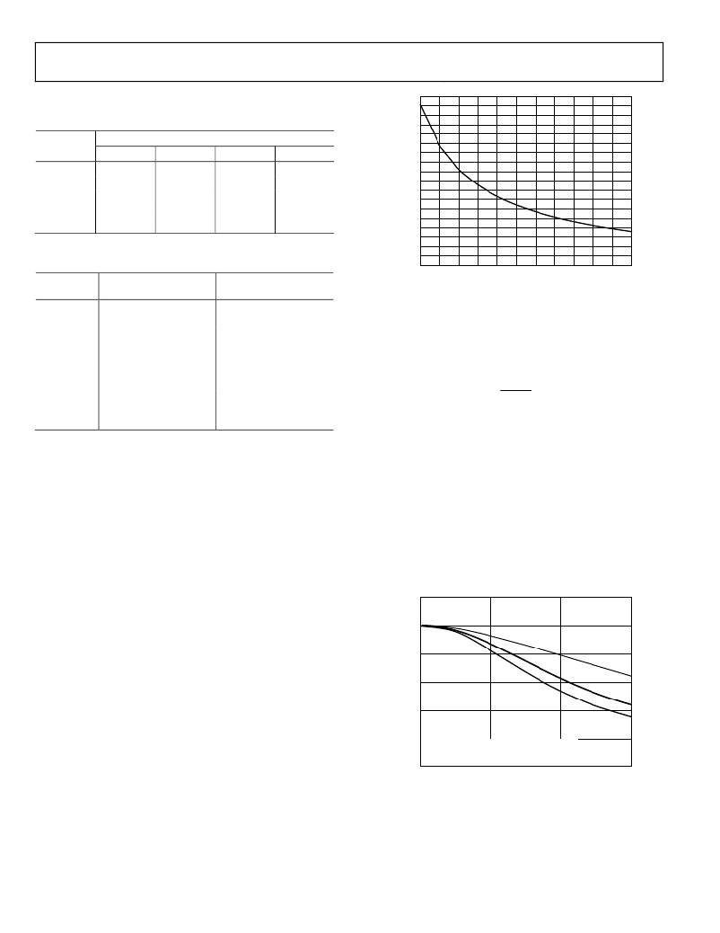
�OUTPUT� CAPACITOR� SELECTION�
�The� output� capacitor� selection� affects� both� the� output� voltage� ripple�
�and� the� loop� dynamics� of� the� converter.� For� a� given� loop� crossover�
�frequency� (the� frequency� at� which� the� loop� gain� drops� to� 0� dB),� the�
�maximum� voltage� transient� excursion� (overshoot)� is� inversely�
�proportional� to� the� value� of� the� output� capacitor.� Therefore,� larger�
�output� capacitors� result� in� improved� load� transient� response.� To�
�minimize� the� effects� of� the� dc-to-dc� converter� switching,� the� cross-�
�over� frequency� of� the� compensation� loop� should� be� less� than� 1/10�
�of� the� switching� frequency.� Higher� crossover� frequency� leads� to�
�faster� settling� time� for� a� load� transient� response,� but� it� can� also�
�cause� ringing� due� to� poor� phase� margin.� Lower� crossover�
�frequency� helps� to� provide� stable� operation� but� needs� large� output�
�capacitors� to� achieve� competitive� overshoot� specifications.�
�2�
�1�
�0�
�15� 20� 25� 30� 35� 40� 45� 50� 55� 60� 65� 70�
�OUTPUT� CAPACITOR� ×� OUTPUT� VOLTAGE� (μC)�
�Figure� 39.� Percentage� Overshoot� for� a� 1� A� Load� Transient� Response� vs.�
�Output� Capacitor� � Output� Voltage�
�For� example,� if� the� desired� 1� A� load� transient� response� (overshoot)�
��Output� Capacitor� ×� Output� Voltage� =� 50� μC�
�50 μ C�
�2� .� 5�
�The� ADP2105/ADP2106/ADP2107� have� been� designed� for�
�operation� with� small� ceramic� output� capacitors� that� have� low�
�ESR� and� ESL.� Therefore,� they� are� comfortably� able� to� meet� tight�
�output� voltage� ripple� specifications.� X5R� or� X7R� dielectrics� are�
�recommended� with� a� voltage� rating� of� 6.3� V� or� 10� V.� Y5V� and� Z5U�
�dielectrics� are� not� recommended,� due� to� their� poor� temperature�
�and� dc� bias� characteristics.� Table� 10� shows� a� list� of� recommended�
�MLCC� capacitors� from� Murata� and� Taiyo� Yuden.�
�When� choosing� output� capacitors,� it� is� also� important� to�
�account� for� the� loss� of� capacitance� due� to� output� voltage� dc� bias.�
��bias� for� three� X5R� MLCC� capacitors� from� Murata.�
�20�
�0�
�Therefore,� the� optimal� crossover� frequency� for� the� control� loop� of�
�ADP2105/ADP2106/ADP2107� is� 80� kHz,� 1/15� of� the� switching�
�–20�
�1�
�frequency.� For� a� crossover� frequency� of� 80� kHz,� Figure� 39� shows�
�the� maximum� output� voltage� excursion� during� a� 1� A� load� transient,�
�as� the� product� of� the� output� voltage� and� the� output� capacitor� is�
�varied.� Choose� the� output� capacitor� based� on� the� desired� load�
�transient� response� and� target� output� voltage.�
�–40�
�–60�
�–80�
�3�
�1� 4.7μF� 0805� X5R� MURATA� GRM21BR61A475K�
�2�
�2� 10μF� 0805� X5R� MURATA� GRM21BR61A106K�
�–100�
�3� 22μF� 0805� X5R� MURATA� GRM21BR60J226M�
�0�
�2�
�4�
�6�
�VOLTAGE� (V� DC� )�
�Figure� 40.� Percentage� Drop-In� Capacitance� vs.� DC� Bias� for� Ceramic�
�Capacitors� (Information� Provided� by� Murata� Corporation)�
�For� example,� to� get� 20� μF� output� capacitance� at� an� output� voltage�
�of� 2.5� V,� based� on� Figure� 40,� as� well� as� to� give� some� margin� for�
�temperature� variance,� a� 22� μF� and� a� 10� μF� capacitor� are� to� be�
�Rev.� D� |� Page� 18� of� 36�
�发布紧急采购,3分钟左右您将得到回复。
相关PDF资料
ECM10DCMN-S288
CONN EDGECARD 20POS .156 EXTEND
ADP2102-4-EVALZ
BOARD EVAL 2.5V-3.3V ADJ OUTPUT
ADP2102-3-EVALZ
BOARD EVAL 1.5V-1.875V ADJ OUTPT
195D685X9020X2T
CAP TANT 6.8UF 20V 10% 2910
195D685X0020X2T
CAP TANT 6.8UF 20V 20% 2910
R1S-1524/H-R
CONV DC/DC 1W 15VIN 24VOUT
195D226X0004X2T
CAP TANT 22UF 4V 20% 2910
A9CAG-0303F
FLEX CABLE - AFG03G/AF03/AFE03T
相关代理商/技术参数
ADP2105ACPZ
制造商:Analog Devices 功能描述:V REG 1A ADJ SMD LFCSP-16 2105
ADP2105ACPZ-1.2-R7
功能描述:IC REG BUCK SYNC 1.2V 1A 16LFCSP RoHS:是 类别:集成电路 (IC) >> PMIC - 稳压器 - DC DC 开关稳压器 系列:- 标准包装:500 系列:- 类型:切换式电容器(充电泵),反相 输出类型:固定 输出数:1 输出电压:-3V 输入电压:2.3 V ~ 5.5 V PWM 型:Burst Mode? 频率 - 开关:900kHz 电流 - 输出:100mA 同步整流器:无 工作温度:-40°C ~ 85°C 安装类型:表面贴装 封装/外壳:SOT-23-6 细型,TSOT-23-6 包装:带卷 (TR) 供应商设备封装:TSOT-23-6 其它名称:LTC1983ES6-3#TRMTR
ADP2105ACPZ-1.5
制造商:Analog Devices 功能描述:V REG 1A 1.5V SMD LFCSP-16 2105
ADP2105ACPZ-1.5-R7
功能描述:IC REG BUCK SYNC 1.5V 1A 16LFCSP RoHS:是 类别:集成电路 (IC) >> PMIC - 稳压器 - DC DC 开关稳压器 系列:- 标准包装:500 系列:- 类型:切换式电容器(充电泵),反相 输出类型:固定 输出数:1 输出电压:-3V 输入电压:2.3 V ~ 5.5 V PWM 型:Burst Mode? 频率 - 开关:900kHz 电流 - 输出:100mA 同步整流器:无 工作温度:-40°C ~ 85°C 安装类型:表面贴装 封装/外壳:SOT-23-6 细型,TSOT-23-6 包装:带卷 (TR) 供应商设备封装:TSOT-23-6 其它名称:LTC1983ES6-3#TRMTR
ADP2105ACPZ-1.8
制造商:Analog Devices 功能描述:V REG 1A 1.8V SMD LFCSP-16 2105
ADP2105ACPZ-1.8-R7
功能描述:IC REG BUCK SYNC 1.8V 1A 16LFCSP RoHS:是 类别:集成电路 (IC) >> PMIC - 稳压器 - DC DC 开关稳压器 系列:- 产品培训模块:Lead (SnPb) Finish for COTS
Obsolescence Mitigation Program 标准包装:50 系列:- 类型:升压(升压) 输出类型:两者兼有 输出数:1 输出电压:5V,2 V ~ 16.5 V 输入电压:2 V ~ 16.5 V PWM 型:- 频率 - 开关:45kHz 电流 - 输出:50mA 同步整流器:无 工作温度:0°C ~ 70°C 安装类型:通孔 封装/外壳:8-DIP(0.300",7.62mm) 包装:管件 供应商设备封装:8-PDIP
ADP2105ACPZ-3.3
制造商:Analog Devices 功能描述:V REG 1A 3.3V SMD LFCSP-16 2105
ADP2105ACPZ-3.3R7
制造商:Rochester Electronics LLC 功能描述: 制造商:Analog Devices 功能描述: